a) Comparison of Raman spectra from WS 2 -only, vertically-stacked
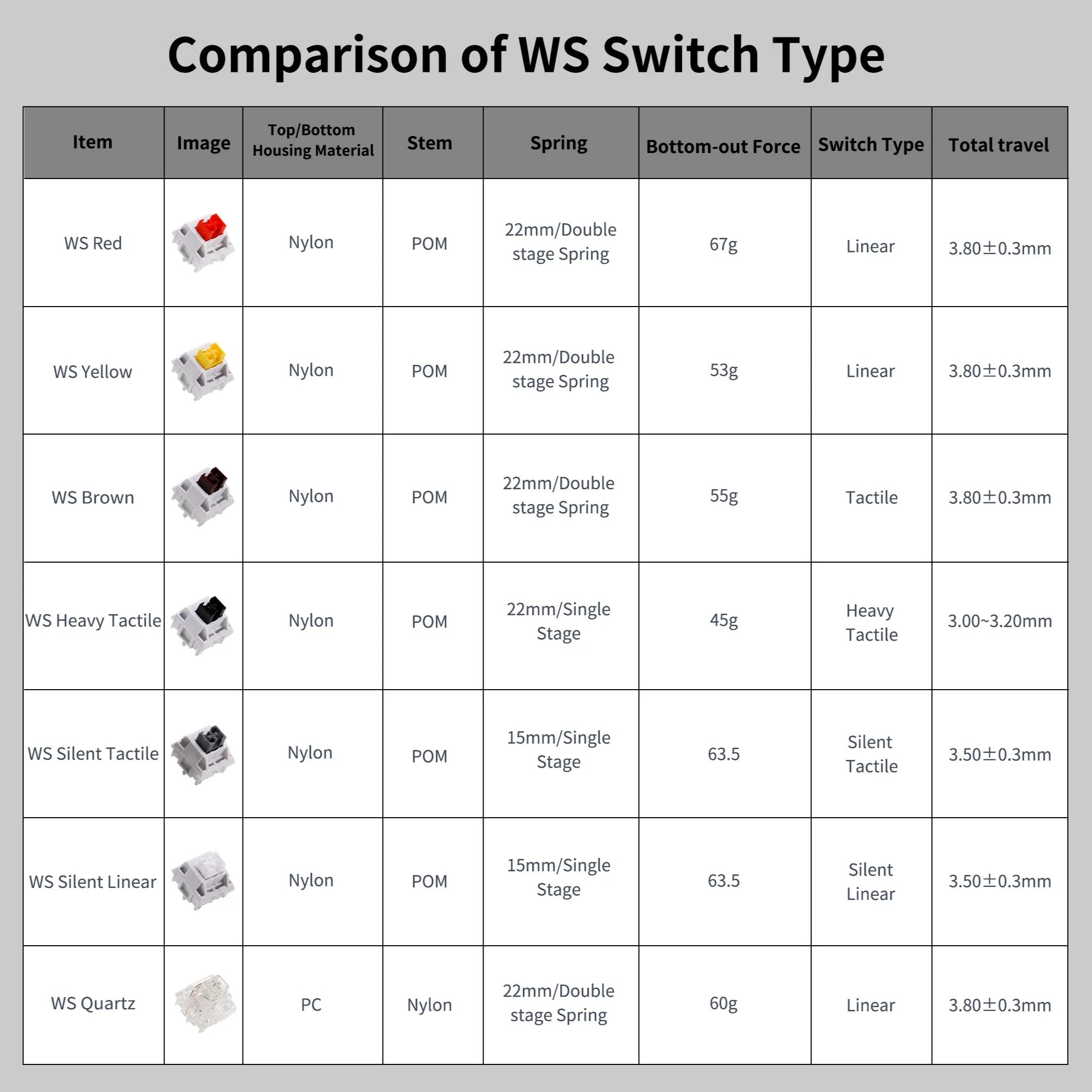
4.9 (119) · $ 10.99 · In stock


PDF] Electronic bandgap manipulation of monolayer WS2 by

Narrowing Bandgap of HfS2 by Te Substitution for Short‐Wavelength
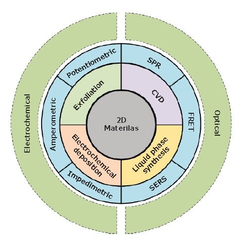
2D Materials Matter: A Perspective on Biosensing Applications
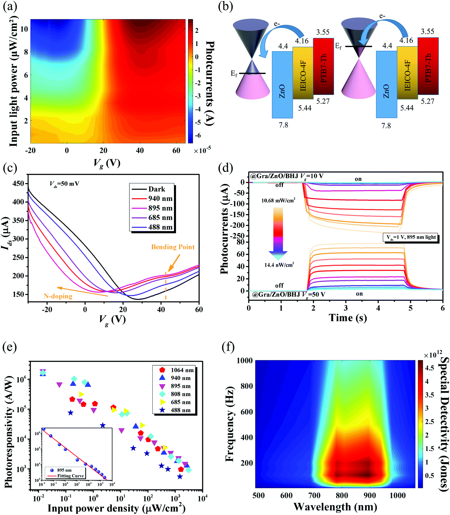
Near-infrared heterojunction field modulated phototransistors with

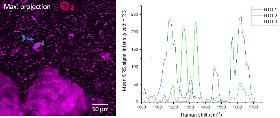
Two-dimensional confocal photoluminescence spectroscopy of

Juhong Park's research works University of North Texas, Texas (UNT) and other places
Formulated Product Characterization with SRS Microscopy

Microscale spectroscopic mapping of defect evolution and filling

PDF) Centimeter Scale Patterned Growth of Vertically Stacked Few Layer Only 2D MoS2/WS2 van der Waals Heterostructure

Fullerene-free, MoTe2 atomic layer blended bulk heterojunctions

Electrical Control of Exciton Diffusion via Tuning Exciton States

Nitin Choudhary's research works University of Central Florida, Florida (UCF) and other places

In (a) we see the Raman spectra of heterostructure MoS 2 /WS 2 and
Recent Advances in Strain-Induced Piezoelectric and Piezoresistive

a) Comparison of Raman spectra from WS 2 -only, vertically-stacked MoS